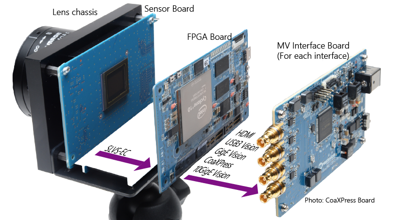
Sony SLVS-EC: You know when you need it! 
Sony’s SLVS-EC Camera Interface (Scalable Low Voltage Signaling with Embedded Clock) has quickly established itself as the future of CMOS Sensor Interfacing replacing SLVS and subLVDS as the interface of choice for high-end designs. Many Sony sensors support SLVS-EC exclusively and even other sensor suppliers are starting to adopt this interface as standard.
| SLVS | SubLVDS | ||||||||||
|---|---|---|---|---|---|---|---|---|---|---|---|
| Effective Data Rate |
|
594 Mbps | 594 Mbps | ||||||||
| Line Coding | 8b10b | None | None | ||||||||
| Lane Configuration | 8 Lanes | 8 Lanes + 1 Clock | 8 Lanes + 1 Clock | ||||||||
| Clocking Method | Embedded Clock | DDR Source-Synchronous Clock | DDR Source-Synchronous Clock | ||||||||
| Differential Signal Level | 200mV | 200mV (160mV min) | 150mV (100mV min) | ||||||||
| Common Signal Level | 200mV | 200mV | 900mV | ||||||||
| Line Termination (TX) | 2 x 50 Ω Single-end | 2 x 50 Ω Single-end | None | ||||||||
| Line Termination (RX) | 100 Ω Differential | 100 Ω Differential | 100 Ω Differential | ||||||||
| Skew Tuning | Do Not Care | Dat /Clock Skew Tuning | Dat /Clock Skew Tuning | ||||||||
| Supply Voltage | 1.2V | 1.2V | 1.8V | ||||||||
| Data Format | Byte Packet | Pixel Packet | Pixel Packet | ||||||||
| H/V Sync | SAV/EAV | SAV/EAV | SAV/EAV | ||||||||
Macnica Mpression: Superior/Proven FPGA IP
Don’t try and re-invent the wheel!
Macnica Mpression has cost-effective, hardware-verified, FPGA-IP for SLVS-EC supporting multiple FPGA suppliers (Intel-PSG preferred, Xilinx option available).
Don’t yoke yourself to an inferior IP partner!
Macnica was first to market with FPGA IP for SLVS-EC v1.2 and first to support SLVS-EC v2.0. Hardware evaluation with Sony IMX420, IMX421, and IMX530 available (EasyMVC). Full details, pricing, documentation, simulation environment, and more under NDA.
EasyMVC
Machine Vision Camera Evaluation/Development Environment available with Sony Sensor Board