
Amazing AZ5H23-02M : How to Evaluate Protection Components for USB Type-C TXRX Short to VBUS
With the rapid advancement of USB application technology, Type-C now enables a compact port to support reversible plug orientation, ultra-high-speed 80 Gbps bidirectional data transmission, multimedia audio/video signal transfer to external displays, and high-power PD power delivery specifications (most commonly 20V/5A). As a result, Type-C has become the standard interface for laptops, smartphones, in-vehicle systems, and high-end electronic devices. However, while this port offers great convenience, it also brings higher challenges in signal integrity and protection design.
Since the USB Type-C port integrates 24 pins within a small 8.6 mm × 2.6 mm area, shorting between adjacent pins is very likely in real applications. This includes power lines and high-speed differential signal lines (TX1-, RX2-, RX1-, TX2-). Once the VBUS pin accidentally contacts a TX/RX pin during hot-plug events, it may cause damage to the ESD protection components on the TX/RX pins, as illustrated in Figure 1 and Figure 2.
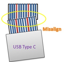
Figure 1. USB Type-C port pin-short example
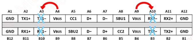
Figure 2. USB Type-C port pinout diagram
Typical scenarios where TX/RX lines may be mistakenly connected to VBUS during hot-plug operations include:
- Connector mechanical mismatch: Long-term use leading to loose ports; unstable contact causes pin wobble and shorts.
- Connector or cable dimensional deviation: Design/manufacturing tolerance by connector vendors, or the use of non-certified third-party cables.
- Environmental dust and moisture: Accumulated dirt or moisture in the usage environment causing conductive contamination.
In these cases, the applied voltage is not a transient ESD event but a sustained DC voltage input, which can easily keep low-voltage ESD protection devices in conduction for long periods, potentially leading to short-circuit failure.
For example, in today’s consumer market, the most common PD voltage is 20V. The most dangerous case is when VBUS (20V) is shorted to a TX/RX pin. If a commonly used TVS with VRWM = 1.5V is deployed, its breakdown voltage is around 5V. Under a sustained 20V VBUS, the TVS will remain conducting and eventually fail (see Figure 3). While choosing a TVS with VRWM > 20V could prevent this issue, such devices typically have very high clamping voltages and thus poor ESD protection performance, often failing ESD qualification. Therefore, in port protection design, it is critical to balance both short-circuit robustness and ESD protection capability. To address this challenge, Amazing Microelectronic has introduced AZ5H23-02M, a device specifically designed for this application scenario.
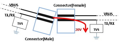
Figure 3. Example of VBUS 20V shorted to TX/RX pin in USB Type-C
To effectively mitigate the above risks while meeting system ESD protection requirements, the device must simultaneously achieve high breakdown voltage, low capacitance, and low clamping voltage. The AZ5H23-02M is the ideal choice:
· High Breakdown Voltage (VBV > 24V)
Unlike conventional 1.5V TVS with a breakdown voltage of 5V, AZ5H23-02M ensures that even under normal PD 20V operation, the device will not inadvertently conduct in a short-circuit scenario. This avoids self-damage and functional failure.
· Ultra-Low Capacitance (CIN = 0.2 pF)
With USB 3.2 data rates reaching up to 10 Gbps, any excessive parasitic capacitance could collapse the eye diagram and degrade signal quality. The AZ5H23-02M’s ultra-low capacitance ensures signal integrity.
· Low Clamping Voltage for True ESD Protection
Although the main scenario here is VBUS shorting, the AZ5H23-02M still provides robust ESD protection during standard IEC61000-4-2 ±8 kV contact discharge. At 8 kV, its clamping voltage (VClamp) is only 10 V, effectively safeguarding the CPU.
· Compact Dual-Channel 0201 Package (0.6 mm × 0.3 mm)
The AZ5H23-02M comes in the same tiny 0201 package as conventional high-speed TVS devices, but supports two channels in one component. This allows protection of two signal lines per device, saving PCB layout space in compact designs. Suggested PCB layouts are shown in Figure 4 and Figure 5.
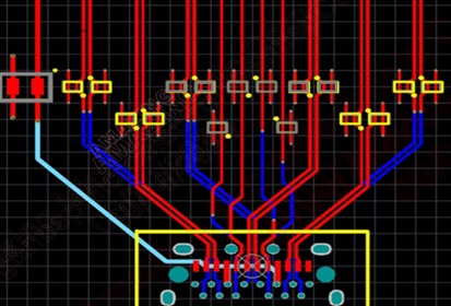
Figure 4. Layout example of single-channel 0201 package
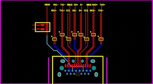
Figure 5. Recommended layout for AZ5H23-02M dual-channel 0201 package
Links
Copyright 2026 Macnica Galaxy International Limited