| Packaging |
- Altera Embedded Multi-die Interconnect Bridge (EMIB) packaging technology
- Multiple devices with identical package footprints allow seamless migration across different device densities
- Mixture of ball pitch FBGA packages, 1,025 mm, 0.92 mm, and several mixed pitch packages
|
| High performance core fabric |
- Second Generation Altera® Hyperflex™ core architecture with Hyper-Registers throughout the interconnect routing and at the inputs of all functional blocks
- Enhanced adaptive logic module (ALM)
- Improved multi-track routing architecture reduces congestion and improves compile times
- Hierarchical core clocking architecture with programmable clock tree synthesis
- Fine-grained partial reconfiguration
|
| Internal memory blocks |
- Multi-level on-chip memory hierarchy
- M20K—20 kilobits with hard error correction code (ECC) support
- MLAB—640-bit distributed LUTRAM
|
|
F-Series
I-Series
|
eSRAM—18 Mb embedded memory block with hard ECC support |
| Variable precision DSP blocks |
- Variable precision DSP blocks with hard IEEE 754-compliant floating-point units, including support for:
- Single-precision FP32 (32-bit arithmetic)
- Half-precision FP16 (16-bit arithmetic) floating point modes
- Tensor floating point FP19 (19-bit arithmetic) floating point modes
- BFLOAT16 floating-point format
- Supports signal processing with precision ranging from 9×9 up to 54×54
- Native 27×27, 18×19, and 9×9 multiplication modes
- 64-bit accumulator and cascade for systolic finite impulse response (FIR) filters
- Internal coefficient memory banks
- Pre-adder/subtractor improves efficiency
- 2× additional pipeline register increases performance and reduces power consumption
|
| Core clock networks |
- Programmable clock tree synthesis—backwards compatible with global, regional and peripheral clock networks
- Synthesize clocks where needed only—minimizes dynamic power
|
| F-Series
I-Series
|
- 800 MHz LVDS interface clocking—supports 1,600 Mbps LVDS interface through the 1.5 V True Differential Signaling (TDS) standard compatible with LVDS, RSDS, mini-LVDS, and LVPECL standards
- 1,600 MHz external memory interface clocking, supports 3,200 Mbps DDR4 interface
|
| M-Series |
- 800 MHz LVDS interface clocking—supports 1,600 Mbps LVDS interface through the 1.3 V TDS standard compatible with LVDS, RSDS, mini-LVDS, and LVPECL standards
- 2,800 MHz external memory interface clocking, supports 5,600 Mbps DDR5 interface
|
| General purpose I/Os |
General |
- Over 700 total GPIOs available
- On-chip termination (OCT)
|
|
F-Series
I series
|
- 1.6 Gbps 1.5 V TDS compatible with LVDS, RSDS, mini-LVDS, and LVPECL standards
- 1.2 V single-ended LVCMOS/LVTTL interfacing
|
|
M-Series
|
- 1.6 Gbps 1.3 V TDS compatible with LVDS, RSDS, mini-LVDS, and LVPECL standards
- 1.05 V, 1.1 V, and 1.2 V single-ended single-ended LVCMOS/LVTTL interfacing
|
|
External memory interface
(Hard IP)
|
F-Series
I-Series
|
1,600 MHz (3,200 Mbps) DDR4 external memory interface |
|
M-Series
|
- 1,600 MHz (3,200 Mbps) DDR4 external memory interface
- 2,800 MHz (5,600 Mbps) DDR5 external memory interface
- 2,750 MHz (5,500 Mbps) LPDDR5 external memory interface
|
| Phase locked loops (PLL) |
I/O PLL |
- Integer PLLs adjacent to general purpose I/Os
- Precision frequency synthesis
- Clock delay compensation
- Zero-delay buffering
- Support external memory and LVDS-compatible interface
|
|
Transmit PLLs
(TX PLLs)
|
- Precise fractional synthesis
- Ultra low jitter with LC tank-based PLL
- Supports transceiver interfaces
|
| Memory controller support |
Multiple hard IP instantiations in each device |
| F-Series
I-Series
|
- DDR4 hard memory controller
- QDR IV using soft memory controller
|
| M-Series |
- DDR5/LPDDR5/DDR4 hard memory controller
- QDRIV support using soft memory controller
- Hard memory network-on-chip (NoC)
|
| High-bandwidth memory |
M-Series |
- In-package HBM2E memory options
- Up to 32 GB of high bandwidth memory
|
| Memory NoC |
M-Series |
- Hardened memory network-on-chip (NoC) enabling high bandwidth data flow between the FPGA fabric and the NoC-attached memories without using FPGA resources
- Supports over 1 TBps of aggregate memory bandwidth
|
| High-performance crypto blocks4 |
- Supports AES and SM4 encryption standards
- Supports GCM and XTS modes of operation
|
| Transceivers |
PCIe* |
P-Tile
F-Tile
|
PCIe* rates up to PCIe* 4.0, 16 Gbps NRZ |
| R-Tile |
- PCIe* rates up to PCIe* 5.0, 32 Gbps NRZ
- Compute Express Link* ( CXL* ) support
|
| Networking |
E-Tile |
- Continuous operating range of 1 Gbps to 28.9 Gbps NRZ and 2 Gbps to 58 Gbps PAM4
- Insertion loss compliant to 802.3bj, CEI 25G-LR, and CEI 56G-LR
- Oversampling capability for data rates below 1 Gbps
- ATX transmit PLLs (LC-PLL) with user-configurable fractional synthesis capability
- XFP, QSFP-DD, OSFP, QSFP or QSFP28, QSFP56, SFP+, SFP28, SFP56, and CFP or CFP2 or CFP4 optical module support
- Adaptive linear and decision feedback equalization
- Transmit pre-emphasis and de-emphasis
- Dynamic partial reconfiguration of individual transceiver channels
- On-chip instrumentation (Eye Viewer non-intrusive data eye monitoring)
|
| F-Tile |
- General purpose transceiver block (FGT) with continuous operating range of 1 Gbps to 32 Gbps NRZ and 20 Gbps to 58 Gbps PAM4
- High speed transceiver block (FHT) with operating ranges of:
- 24 Gbps to 29 Gbps NRZ and PAM4
- 48 Gbps to 58 Gbps NRZ and PAM4
- 96 Gbps to 116 Gbps PAM4
- The F-Tiles in these devices have the following transceivers:
- I-Series—FHT and FGT transceivers
- M-Series—FHT and FGT transceivers
- F-Series—FGT transceivers only
|
| Transceiver hard IP |
PCIe* |
Multiple hard IP instantiations in each device |
|
P-Tile
F-Tile
|
- Up to PCIe* 4.0 ×16 EP and RP
- Port bifurcation support: 2×8 endpoint or 4×4 root port
- TL bypass feature
- Single-root I/O virtualization (SR-IOV): 8 physical functions or 2K virtual functions
- VirtIO support
- Scalable IOV
- Shared virtual memory
|
| R-Tile |
- Up to PCIe* 5.0 ×16 EP and RP
- Port bifurcation support: 2×8 endpoint or 4×4 root port
- TL bypass Feature
- SR-IOV: 8 physical functions or 2K virtual functions
- VirtIO support
- Scalable IOV
- Shared Virtual Memory
- PIPE Direct mode
- Precise Time Management
|
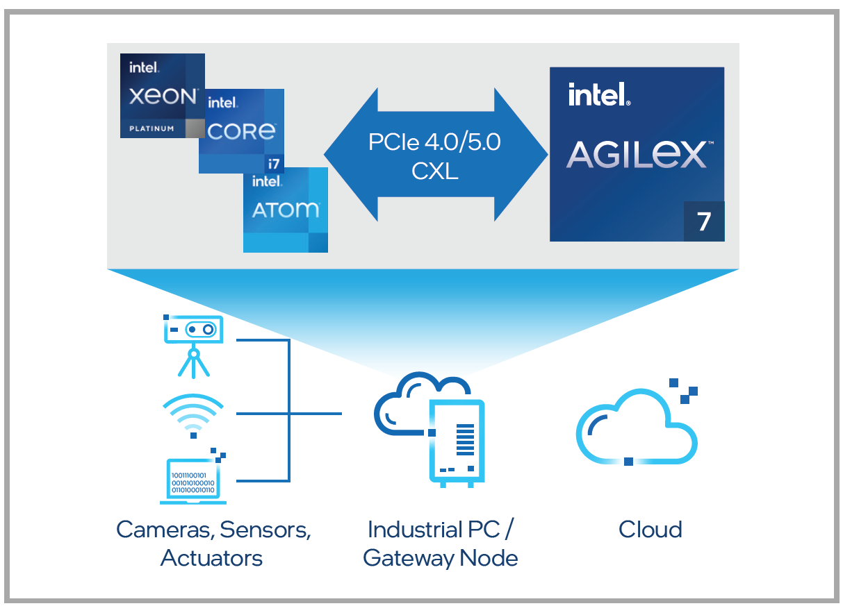
| CXL* |
R-Tile |
- Up to PCIe* 5.0 ×16 EP
- Selected features support CXL* 1.1 and 2.0 specifications
- Soft logic (encrypted) to support CXL* Type 1, Type 2, or Type 3 devices
- Mix and manage different memory types and controllers
|
| Other protocols |
E-Tile |
- Ethernet IP configurations:
- 24× 10 or 25 GbE MAC, PCS, and RS-FEC
- 4× 100 GbE MAC, PCS, and RS-FEC
- CPRI and fibre channel FECs
- CR/KR (AN/LT)
- 1588 PTP
- MAC, PCS, and FEC bypass options
- PMA Direct Mode
|
| F-Tile |
- Ethernet IP Configurations:
- 16× 10 or 25 GbE MAC, PCS, and FEC
- 8× 50 GbE MAC, PCS, and FEC
- 8× 40 GbE MAC, PCS, and FEC
- 4× 100 GbE MAC, PCS, and FEC
- 1× 400 GbE MAC, PCS, and FEC
- KP FEC support
- Flex-O FEC, FlexE PCS and FEC, Ethernet over OTN Mode, SyncE, fibre channel, and CPRI FEC
- CR/KR (AN/LT)
- 1588 PTP
- MAC, PCS, and FEC bypass options
- PMA Direct Mode
|
| Configuration |
- Dedicated SDM
- Software-programmable device configuration
- Fine-grained partial reconfiguration of core fabric—add or remove system logic while the device is operating
- Dynamic reconfiguration of transceivers and PLLs
- PUF service
- Platform attestation
- Anti-tamper features
|
| F-Series |
- Serial and parallel flash interface
- Configuration via protocol (CvP) using PCIe* 1.0, 2.0, 3.0, or 4.0
- Comprehensive set of security features including AES-256, SHA-256/384, ECDSA-256/384 accelerators, and multi-factor authentication
|
|
I-Series
M-Series
|
- Serial and parallel flash interface
- Configuration via protocol (CvP) using PCIe* 1.0, 2.0, 3.0, 4.0, or 5.0
- Comprehensive set of security features including AES-256, SHA-256/384, ECDSA-256/384 accelerators, and multi-factor authentication
|
| Software and tools |
- Altera ® Quartus® Prime Pro Edition design suite with new compiler and Hyper-Aware design flow
- New compile innovations in each Altera® oneAPI release
- Transceiver toolkit
- Platform Designer IP integration tool
- Altera® DSP Builder for Intel® FPGAs advanced blockset
- Arm* Development Studio for Altera® SoC FPGA (Arm* DS for Altera® SoC FPGA)
|