
Outstanding OIP2 from a Small Dual MMIC Amplifier

To say that the push-pull amplifier has been around a while, and that its second order distortion benefits have been understood for a period of time are both gross understatements. Edwin Henry Colpitts of Western Electric Company was awarded Patent No. 1,128,292 on February 1, 1915 for an “electric wave amplifier” in which he connected two vacuum tubes together in a push-pull configuration and recognized that this configuration “[avoids] a certain amount of distortion in the output waves.”1,2
More than 110 years later, we find push-pull amplifiers everywhere, from the high-power, broadband transmitter path to low level, sensitive, multi-octave receiver applications. The technological changes that have occurred over 110 years are numerous, but perhaps the most astonishing is the miniaturization that has taken place. In this article we explore a tiny, wideband push-pull amplifier solution that runs from HF to the lower UHF frequency range, achieving an OIP2 of nearly +100 dBm along the way. The centerpiece of this ultra-high linearity solution is the Mini-Circuits’ PHA2-13HLN+dual matched pair.
The Basic Building Blocks – Pushing, Pulling, and Second Order Cancellation
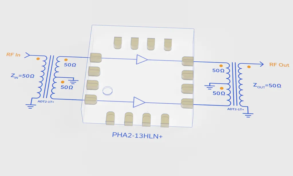
The traditional configuration of a push-pull amplifier stage is shown in Figure 1. It is comprised of an amplifier stage, in this case the PHA2-13HLN+ dual matched pair, and an input and output balun transformer. The input and output transformers are impedance-matched to 50Ω to meet the amplifier requirements. The input transformer steps up from 50 to 100Ω (1:2 impedance ratio and 1:1.41 turns ratio) and is then center-tapped, while the output transformer steps down from a center-tapped 100Ω to 50Ω (2:1 impedance ratio and 1.41:1 turns ratio). Each transformer leg presents the appropriate 50Ω impedance to maintain proper matching throughout the signal path.
The secondary of the input transformer, center-tapped to yield a pair of 50Ω windings, enables the PHA2-13HLN+ dual amplifier input to operate push-pull with very little additional impedance matching. Likewise, the amplifier outputs can each drive their end of the split primary of the now-mirrored balun transformer directly, since each of the windings is 50Ω. To examine how the push-pull action is sustained, follow the balun transformer dot convention.
Figure 1: Traditional push-pull configuration amplifier using 2:1 (impedance ratio) balun transformers.
As the single-ended (unbalanced) input swings to its maximum positive voltage, so does the upper amplifier in the pair, while the lower amplifier simultaneously swings to its lowest input voltage. As the single-ended input swings to its lowest point, so does the input to the upper amplifier, while the lower amplifier swings to its maximum positive input. This pushing and pulling action that begins at the input follows through the amplifiers, and into the output transformer where these two opposing amplifier signals are recombined by the output balun transformer. While the fundamental signals are differentially combined after a 180⁰ phase inversion, OIP2 cancellation occurs because second harmonic distortion occurring at a frequency of 2f0 is not inverted (shifted 180⁰) by the transformer baluns, and instead appears in-phase (shifted 360°, or unaffected) across the baluns, making them common-mode signals that are rejected during recombination. In essence, signals at 2f0 simply get cancelled out (technically, become common mode, and get rejected) in their attempt to utilize the balun transformer to split or recombine.
Similarly, second-order intermodulation distortion products occurring at frequencies f₁ + f₂ and |f₁ – f₂| for two-tone inputs take advantage of this 2nd order rejection (most often referred to as “cancellation”) as the basis for why the push-pull amplifier exhibits such a significant benefit over the traditional, wideband, single-ended amplifier.
The Detailed Circuit Board Schematic
The complete test board schematic for the TB-PHA2-13HLNC+ is shown in Figure 2 and the associated parts list in Table 1. Note first that input of wideband balun transformer T1 and the output of T2 are on the non-dot side of the transformer. While they may also be connected to the dot side (arguably the more common way of illustrating push-pull operation) as well, RF-IN and RF-OUT must connect to like ends (polarities) of the balun transformer. To achieve wide bandwidth (well over a decade) and low loss at relatively low frequencies (10 to 500 MHz), core-and-wire ADT2-1T+ transformers are utilized. R1 and R2 provide negative feedback to broaden the bandwidth, and to also flatten the gain from 10 to 500 MHz.
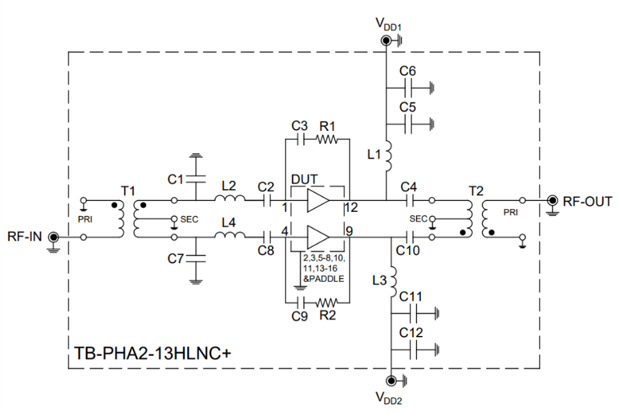
Figure 2: Schematic diagram for the push-pull circuit utilizing the PHA2-13HLN+ dual matched amplifier (TB-PHA2-13HLNC+)
Their associated capacitors C3 and C9 block drain bias from being fed back to the RF input terminal of the PHA2-13HLN+. C1/L2 and C7/L4 are for impedance matching and C2, C4, C8, and C10 are DC blocking capacitors. Decoupling capacitors C5, C6, C11, and C12 filter VDD before it reaches the amplifier bias terminals by way of RF chokes L1 and L3. The DUT is the PHA2-13HLN+ dual amplifier, as shown.
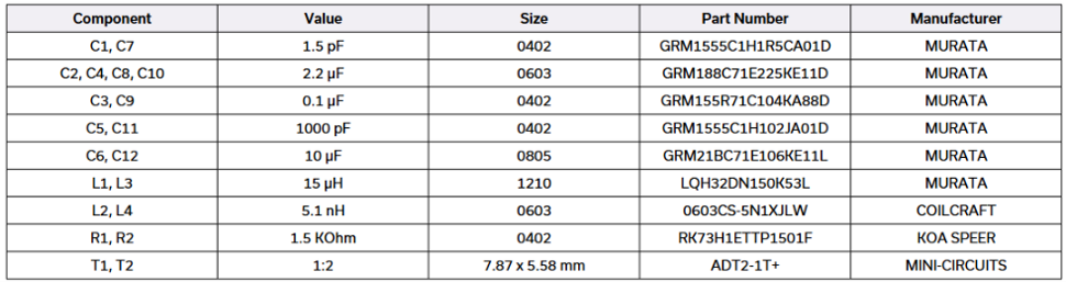
Table 1: List of component reference designators, descriptions and part numbers associated with test board TB-PHA2-13HLNC+
Hitting 100 in Seconds – OIP2 Performance
The PHA2-13HLN+ dual matched amplifier, configured as shown in Figure 2 and Table 1 was measured by Mini-Circuits for OIP2 performance, and the results were outstanding. As the paragraph title suggests, we did hit +100 [dBm] in “seconds” (output second order intercept points, or OIP2) for two of the five test boards characterized. Before we leaned too far forward on our skis, though, we first established a single-ended baseline by plotting OIP2 for a single PHA-13LN+ at 5V, as shown in Figure 3. The single-ended device achieves over +60 dBm out to 50 MHz, peaking at just over +70 dBm, then flattens to approximately the mid +50 dBm range out to a frequency of 500 MHz.
The curve at the top of the chart for a blended average of five dual matched test boards (TB-PHA2-13HLNC+) is nothing short of excellent. The dual matched amplifier version is comprised of two single-ended devices harvested off the wafer in very close proximity to one another in order that the devices closely match in terms of gain and insertion phase and to optimize second order cancellation. As stated previously, two test boards breached the +100 dBm mark, and the average tops out at +99 dBm. Most impressive is the sheer bandwidth of the cancellation that leads to such high OIP2 performance. The curve at the bottom of Figure 3 is the level of cancellation of second order products necessary to achieve such great OIP2 performance. Note that we achieve over 5 octaves (more than 1.5 decades) of 20 dB or more cancellation (10 to 340 MHz) and greater than 3 octaves of 30 dB or more (~26 to ~210 MHz ).
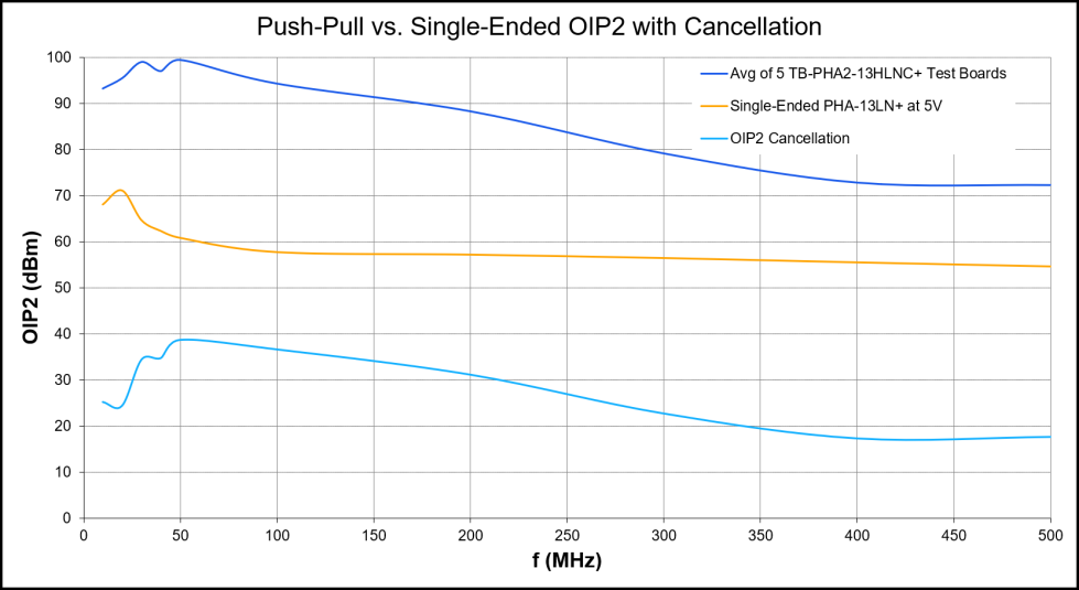
Figure 3: OIP2 comparison between single-ended PHA-13LN+ and push-pull PHA2-13HLN+ showing net OIP2 cancellation.
Mini-Circuits Doesn’t Get Pushed Around
The push-pull amplifier and second order cancellation are literally second nature to Mini-Circuits, and we have written extensively on the subject.3,4 In this article, we reviewed the push-pull topology and how second order cancellation is realized through its implementation. We reviewed the circuit details of Mini-Circuits’ test board that employs the PHA2-13HLN+ dual matched amplifier. Ultimately, we exhibited the impressive OIP2 performance of a blended average of five (5) TB-PHA-13HLNC+ test boards overlayed with single-ended performance from the PHA-13LN+ amplifier. The difference between the two OIP2 curves (cancellation) was plotted separately and analyzed. The results were 20 dB or more cancellation over a decade of BW and 30 dB or more cancellation over 3 octaves. When push comes to shove, Mini-Circuits can achieve impressive linearity.
參考資料
1. Edwin Henry Colpitts, Electric Wave Amplifier, US1128292A – Electric-wave amplifier. – Google Patents
2. WESTERN ELECTRIC CO., Inc., et al., v. WALLERSTEIN. Circuit Court of Appeals, Second Circuit. July 18, 1932. WESTERN ELECTRIC CO. v. W | 60 F.2d 723 (1932) | 0f2d7231537 | Leagle.com
3. https://blog.minicircuits.com/understanding-rf-microwave-push-pull-amplifier-design/
洽詢安馳科技:marketing.anstek@macnica.com
Links
Follow us on ANStek social channels
Related Site
ADI Product Microsite | ANStekADI.com
ANStek Web Portal | Linktree
©Copyright 2026 Macnica Anstek Inc.