
AB20-U2PCI
- Product Image
Convert a PCIe x16 edge connector into four U.2 or U.3 NVMe ports to evaluate multi-drive NVMe designs on FPGA platforms.
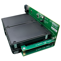
AB20-U2PCI lets you attach up to four 2.5 inch U.2 or U.3 NVMe SSDs to an FPGA board through a single x16 PCIe slot. The board integrates a low-jitter reference clock and reset circuitry so NVMe evaluation is stable at high PCIe rates.
Highlights
- Four U.2 or U.3 ports on the component side, one PCIe x16 connector on the solder side
- Internal lane mapping splits x16 into four x4 links for four independent SSDs
- Onboard low-jitter clock generation and reset distribution for reliable bring up
- Designed for multi-drive NVMe IP evaluation and prototype development
Why Macnica?
- We map SSD topologies and lane splits to your target throughput and endurance goals
- Proven Agilex evaluation flows and adapter cabling so lab bring up is repeatable
- Guidance on thermals, power budget, and fan choices for sustained runs

Key Specifications
- PCIe lanes: x16 host connector, four x4 ports to SSDs
- Drive support: U.2 or U.3 NVMe SSDs, up to four
- Clocking: Onboard reference clock for PCIe and SSDs
- Use with: NVMe-IP family, NVMeTCP-IP, and related storage flows
Typical Applications
- Multi-SSD NVMe capture and replay testbeds
- NVMe RAID-style experiments on FPGA platforms
- Storage front ends for high-rate data movers
Resources
Get Started
Tell us your SSD count, form factor, and sustained write target. We will propose a lane plan, cables, and a validated demo flow.
Similar Products
Macnica Americas Site Map


©Copyright 2026 Macnica Americas, Inc.