
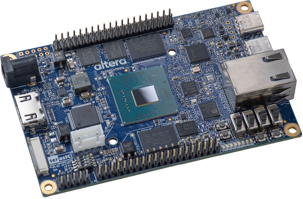
Terasic DE25-Nano Development and Education Platform

The Terasic DE25-Nano uses the Agilex A5EB013BB23B SoC FPGA which increases the available FPGA logic to 138KLE and 8.42Mbits of embedded memory. The MicroSD Card Socket, 2x20 GPIO headers, 8-channel ADC, accelerometer, gigabit Ethernet and HDMI 1.4 output maintains backwards compatibility with legacy DE10-Standard applications. With the addition of the MIPI CSI camera interface, a second 1 GB bank of high-speed LPDDR4 memory and 188 on-FPGA tensor blocks (up to 5.78 INT8 TOPS), the DE25-Nano is an excellent development platform for edge AI and machine vision applications.
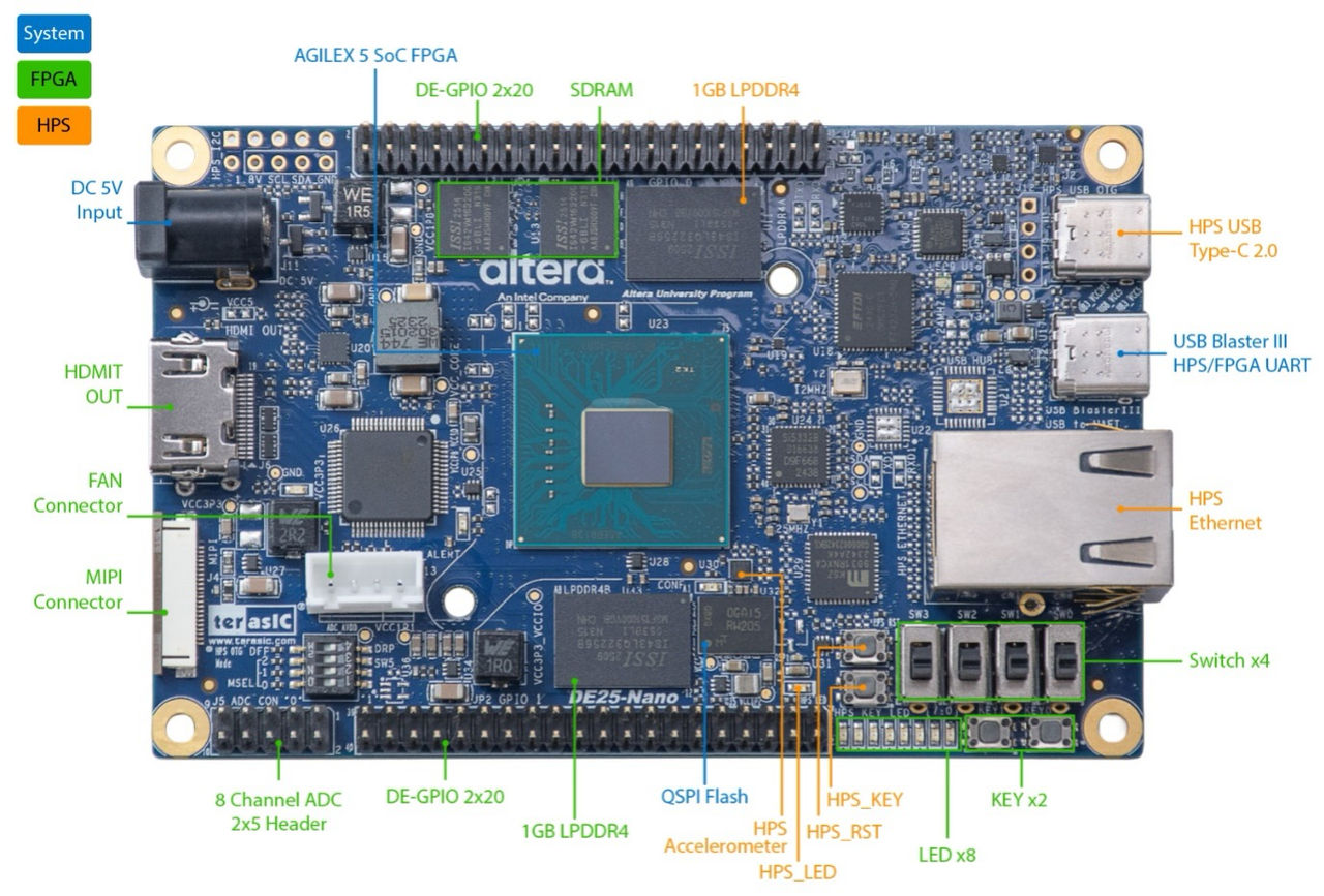
The integrated ARM cores have been upgraded to dual ARM Cortex A76 cores and dual ARM Cortex A55 cores operating up to 1.4GHz and 1.25GHz, respectively. This heterogenous ARM architecture permits the Cortex A76 cores to handle the application-level tasks while the Cortex A55 cores handle the real-time hardware management tasks. The ARM cores (HPS) are connected to 1 GB of external LPDDR4 memory which can shared with the FPGA. The HPS peripheral connectors include the RJ45 Gigabit Ethernet, UART to USB, MicroSD socket and an USB Type-C host port. An onboard USB Blaster III interface is included to permit immediate FPGA and application code development.
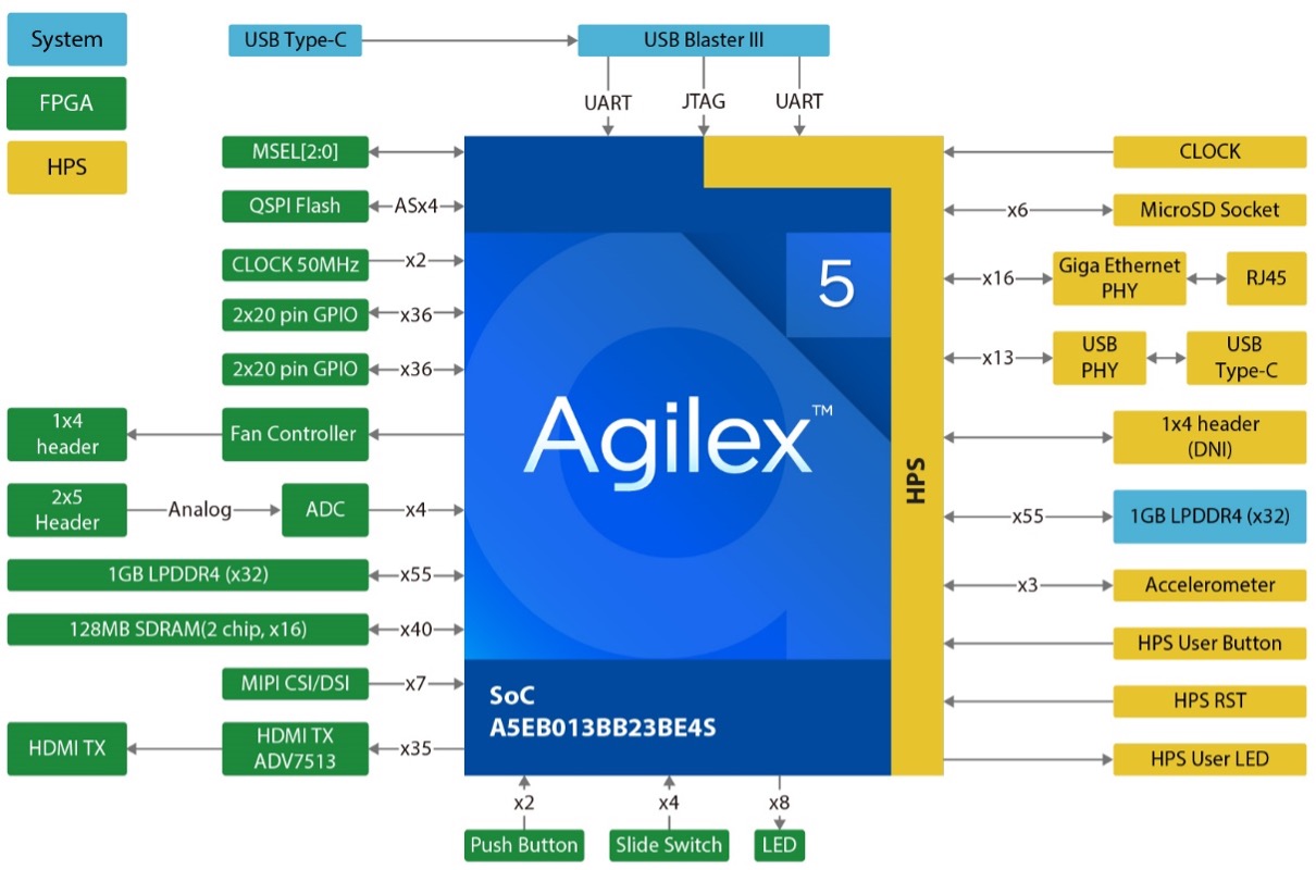
Block Diagram
The DE25-Nano is supported by an extensive set of documentation enabling new and seasoned designers to quickly build and integrate this platform into their projects and prototypes. The Golden Hard Reference Design and several clearly documented FPGA design examples such as a Sony MIPI camera demo are available from the Terasic website. Additionally, a comprehensive Linux build and instructions on how to build the Linux kernel from scratch are available from the DE25-Nano Github page. The Terasic DE25-Nano is in stock and available for immediate delivery.
Target Markets
- Education
- Robotics
- AI and Machine Vision
- Industrial and Embedded Systems
- Test and Measurement
Macnica Americas Site Map


©Copyright 2026 Macnica Americas, Inc.